Brainstorming a Modern Retro Console, Part 1
In which the author channels his inner mad scientist and lays out ideas for a modern, retro-built video game console, beginning with part 1: the 65xx-based multiprocessor CPU array.
By: TheHans255
4/5/2024
It's time for some mad-scientist project ideas! A few weeks ago, the work I've been doing with the MOS 6502 gave me some inspiration for a modern retro console design that uses the processor, much like the NES and other consoles of the 1980s. I thought: if I wanted to build something that would carry the same design ethos as those consoles, with retro processors and bespoke graphics and audio hardware, yet had the benefit of modern technology and wanted to build something that made more unique and capable games than those original consoles could, what would I build?
Ideally, of course, I would build this design myself, but since I have such a huge backlog of projects, and this particular project requires both several FPGAs and knowledge of Verilog that I haven't really used since college, I thought I might post these ideas and plans to the Internet instead, so that I can share some of my software engineering thoughts about these designs and hopefully inspire someone to go forward and build!
This article comes in 4 parts:
- This, the first part, is about the 6502 processor and memory array.
- The second part is about the GPU, a rasterizer specifically optimized for these low-spec processors.
- The third part is about the cartridge interface and the BIOS,
- The fourth part is about the other components, such as the audio driver and controller.
All of these components are more or less independent ideas, especially the first and second parts, so feel free to mix and match for your own creations!
(And of course, all of this comes with a disclaimer: I have not built or tested any of this. All of this comes from my knowledge of the 6502 and other electrical engineering that I have picked up passively over the years, and while I believe that these designs would work to the best of my knowledge, I provide no warranty on any of these designs' effectiveness or their safety in mission critical systems. If I ever get around to physically building these designs, I will update this article with my results.)
Background: The WDC65C02 Processor
First, a quick primer about the main processor we intend to use, the 6502 processor. Or, more specifically, it's CMOS-based 65C02 variant. Why would we want to use it, and what benefits does it provide us as console designers?
The 65C02 processor (full name WDC65C02), is an 8-bit microprocessor that's been around since the early 1980s. It is fully compatible with the original NMOS 65xx line, the chips that powered the Atari 2600, NES, Apple II, Commodore 64, and others, and can run at the same speeds and specs (1.1 MHz, 16 address lines, 8 data lines, 8-bit arithmetic, binary-coded decimal mode), meaning that developers used to those 65xx-based systems can transition more readily to a system using this chip. However, this model has several advantages over the original 6502:
- The processor uses CMOS (Complementary Metal Oxide Semiconductor) instead of NMOS (N-channel Metal Oxide Semiconductor) technology for building its transistors and other logic. This is useful in plenty of ways, such as power savings, but of particular use to this project is that the CPU can be run at arbitrary and irregular clock speeds, ranging anywhere from 14 MHz all the way down to individual clock pulses at the press of a button (the NMOS variant, on the other hand, starts to deterioriate when you go below 10,000 Hz).
- As mentioned, the processor can operate at up to 14 MHz, while the NMOS processor only gets up to about 1 MHz. This allows up to 14 times more processing power in the same time frame.
- A few additional instructions are available (such as the "BRA", or BRanch Always instruction, as well as the "STP" (SToP) and "WAI" (WAIt) instructions), and a few instructions and operating modes have had bug fixes. In addition, the "undocumented instructions" of the 6502 (which essentially did multiple operations at once and sometimes locked up the processor) are now NOP (no-op) instructions.
- Unlike the NMOS 6502, you can still, as of this writing, buy new 65C02 processors today, at less than 10 USD a pop.
And for that 10 USD a pop, what kind of processor do you get? A processor that can access 64 KiB of memory and other devices, 8 bits at a time, at a rate of up to 14 million times per second (or really 7 million times, considering that most instructions take at least 2 cycles to complete). It can read write memory to a handful of registers, do addition and subtraction, and jump/branch/call code with a 256-byte stack. Absolutely nothing compared to what modern x86_64 or ARM processors can do today, but nothing to sneeze at for the value either. And since any of those 64 KiB of "memory" addresses can actually be wired to any device that responds well to the 65C02's 5 volt signals, it can easily operate many devices and support endless hardware configurations.
Making A 6502 Frankenstein
Now for the fun part - since you've been primed on what the 65C02 is, we can talk about what we're going to do with it: strap a bunch of them together in a demented attempt to let them run multithreaded code!
Since the late 2000s saw a decrease in the raw speed we could give to modern CPUs (which have been stuck between 2 and 4 GHz for over a decade), chip manufacturers instead responded by stuffing multiple "cores" into the same chip, each one being a separate processor that could run code at the same time as the other processors next to it. Writing code to take advantage of multiple processors is harder than writing traditional, single-threaded code, but it allowed much more raw power than what a single processor could provide, and also lays the groundwork for potentially orchestrating far more distributed computing power across a network like the Internet. It stands to reason, that the same principle could be applied to these low-power CPUs as well, and developers could get more raw power with multiple, independent processors at their fingertips.
The 6502 has not had much historical precedent for sharing the same memory across multiple instances of itself - most devices that use a 6502 or 65C02 use only one. However, several 65xx-based devices, such as the Apple II, do have a history of sharing the same RAM with another device: the video controller. Everything in the Apple II - the CPU, the RAM, and the video controller - would run off the same overarching clock, and the CPU and the video controller would take turns, one cycle at a time, accessing the RAM to either modify memory or generate the output image. We will use this same principle to orchestrate our 65C02 processors - each of them will take turns with a central bank of public RAM, each running at their own individual clock speeds while the RAM runs at that speed times the number of CPUs we orchestrate this way.
To show an example of what I mean by this, let's say that an array of 3 processors is running this 65C02 assembly code below:
1000: LDX #$00
1002: LDA $2000,X
1004: CMP #$80
1006: BEQ $1010
1008: INX
1009: BNE $1002
Each processor has its own internal state that puts it at different parts of
the program, yet all of them share the same memory, including both this program
and the $2000 that it is reading from.
- A clock cycle begins on the RAM and on processor 1 (the clock lines on processors
2 and 3 are unchanged). Processor 1 has its Program Counter set to
$1008and is at the instruction fetch step, so it interacts with the RAM to fetch the byte at$1008. It retrieves the byte for theINXinstruction and sets itself up to execute that instruction on the next cycle, also incrementing its program counter. - The clock cycle ends, and both the processor and RAM rest.
- Another clock cycle begins, this time on the RAM and on processor 2 (the clock lines
on processors 1 and 3 remain unchanged). The processor has its Program Counter set
to
$1000- it has just entered the subroutine - and is also in the instruction fetch phase. It retrieves the byte for the Immediate-modeLDXinstruction and sets itself up to execute that instruction, also incrementing its program counter. - The clock cycle ends again.
- Another clock cycle begins, this time on the RAM and on processor 3. This processor
has its program counter set to
$1006, but this time is performing the last step of theCMPinstruction at$1004. This involves subtracting$80from the value it has already stored in the accumulator (let's say it's$7F, though that doesn't matter for this example) and setting the resulting processor status flags. - The clock cycle ends again.
- Yet another clock cycle begins, this time on RAM and processor 1 again. The processor
has its program counter set to
$1009, but is ready to execute theINXinstruction. It increments its internal X register (which is separate than those of the other two processors), and sets the flags. - The above cycle continues, with each processor processing and executing instructions in turn. At any given time, at most one of them has full control of the public memory, meaning that all accesses will remain coherent as if only one processor was accessing them.
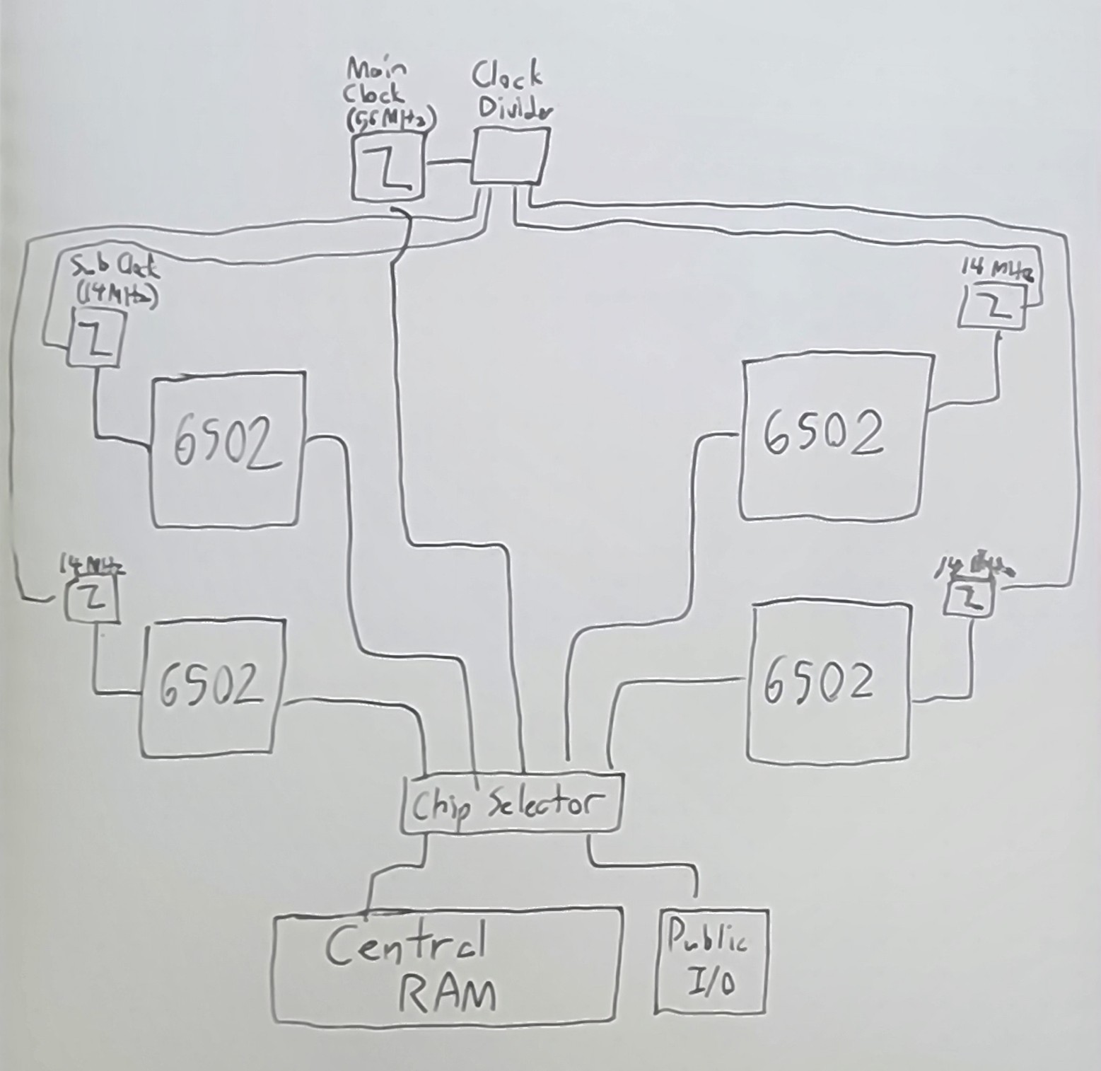
The actual full clock speed would either be 14 MHz times the number of processors, or the maximum speed supported by the central RAM chips, whichever is slower. Any number of other devices that need access to the public RAM, such as a video controller, can also take turns as needed in this Round Robin configuration.
As for what exactly is in the central memory, it could really be anything you want, just
as it would with any other 6502-based design. A good chunk of it would likely be RAM,
though it would also necessarily include some ROM to initialize your processors (both
including the interrupt vectors at $FFFA-FFFF as well as code to get the system moving),
and may also include some memory-mapped IO to control external devices.
Making it Practical with Private Memory
While the above likely works in principle, it would not be practical from an actual system design standpoint, since there is more state than just the internal processor registers that would need to be kept separate between systems. In particular:
- There must be a way for the different processors in the array to identify themselves.
This can just be a single byte (e.g. the bytes
$01through$04for each processor), but we have to ensure that it is read differently so that each processor can branch to its own part of the program. And since there is no dedicated way in the 65C02 to directly set the program registers, this should be accomplished through a memory address. - Unless we want to (rather hopelessly) juggle multiple tiny stacks in the
$0100-0FFFstack page, each processor will need its own range of RAM in that page so that it can call subroutines and keep track of return/stack values independently of the other processors. - The "zero page" (
$0000-00FF) is a special range of memory for the 6502 processor. Most of the core instruction set (e.g. load/store, jump, compare, etc.) have smaller variants that specifically target zero page (by omitting the leading$00from memory), and there are some instructions, such as jumping through a function pointer, that only work with operands stored in zero page. As such, zero page can be thought of as a set of extended registers in their own right, and the processors will likely function better if this range is kept separate.
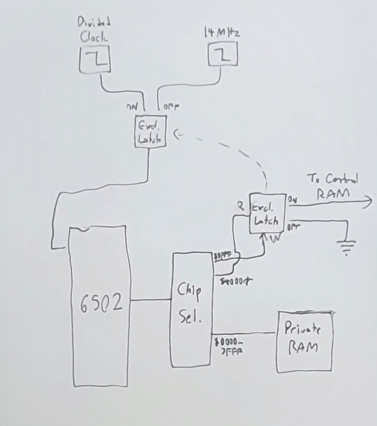
All of these issues can be solved by wiring a small bank of "private memory" to each processor - for addresses below a certain threshold, memory accesses will instead go to this local memory chip instead of the public chips. This memory will be at least 512 bytes to contain the zero page and stack pages, and could contain much more depending on the needs of the system (perhaps up to 16 KB). Somewhere in that area, a single address would instead go to a read-only contraption that gives the processor its identifying number, allowing it to take whichever path it needs to in order to start following orders.
Beyond this, the private memory area can be also designed any way you want, much in the same way the central memory is designed (besides the fact that you would probably not include any ROM besides the chip identifier). This can allow you to control various thread-local or processor-exclusive devices, such as giving each processor a co-processor or serial communications line, or giving one processor exclusive access to the audio controller or external storage media.
Accelerating Processing with Private-Exclusive Mode
With this setup in place, we are already well on our way to a multithreading capable 65C02 system. However, if we're operating on a system where our shared clock speed is limited by the central public memory, we are still limited from reaching the full potential of each processor. Therefore, if a processor doesn't need access to the central memory and can do its processing just fine on its own private memory, then it should be welcome to do so and go up to its full speed without disturbing central memory.
We will do this by including a soft switch in each processor's private memory that allows it to switch between a shared mode and a full speed mode, which the processor can manipulate by accessing two side-by-side memory addresses.
- When the processor is in shared mode (as is default), it participates in the Round Robin cycle detailed above, syncing its clock to the public memory and limiting itself to its clock speed. The processor will also receive interrupts (such as the NMI, usually used to signal VSync/VBlank) as normal.
- When the processor is in full speed mode, it disconnects from the Round Robin
cycle and instead runs at a full 14 MHz clock along with its private memory
hardware. It is disconnected from central memory, and any attempts to access
it are undefined. Interrupts are also disabled (since the interrupt vectors stored
in
$FFFA-FFFFaren't accessible anymore). During what would otherwise be that processor's turn, the Round Robin cycle will run a clock cycle on the central RAM and perform a dummy read at some undetermined address.
It is likely that the process to switch from one to the other would be a several-cycle process, in which time the processor cannot expect any strict wall-clock timing to its instructions and should not access central memory until the process is complete. If this takes an indeterminate amount of time, the processor would also benefit from a memory-mapped IO address that tells it whether it is connected to central memory.
The primary use of this acceleration mode would be complex batch processing - a processor could, for instance, copy a set of game objects into its private RAM, switch into full-speed to run an O(n2) collision check or sorting operation on them, then go back into shared mode to copy the results back into central RAM. A processor might also put itself into full speed mode in order to perform a timing critical operation - for instance, load an audio sample into private RAM and go into full-speed to play it, knowing that interrupts would not mess up the timing.
Other Notes and Limitations
- We would largely be free to control interrupts however we wanted. NMI would likely
be used for VBlank, as it is on the NES. Maskable interrupts would likely be
best used to implement condition variables,
which allow multiple processors to efficiently wait on others to finish tasks -
the 65C02's
WAIinstruction allows the processor to sleep until the next interrupt occurs, which interrupt would be triggered by whichever other processor it was waiting on. - The RESET signal would only come with a full reset of the system (i.e. it would not have the state-preserving "Warm Start" behavior of the Apple II). The processors would wake up from RESET only after all external devices have been reset to their default state, central memory has been mapped to include the appropriate startup ROM (including the RESET vector), and all processors have been set back to the shared execution mode.
- This processor system is designed for improved parallelism and concurrency, but is designed with the notion that a single programmer still has control over all code running on the system - as such, it is not designed for process isolation, especially of the kind implemented by modern OSes where user code is kept separate from kernel code and where the kernel prevents the user from messing the system up.
- If the console supports remapping of the central memory, it will have to be very careful to make sure that this remapping is synced correctly with the other processors and that other processors are not going to fail catastrophically if the memory pages are changed. For this reason, it is likely that this console would need to remap very rarely, perhaps only once for each major game mode, and if it needed to access a larger space more than that, it would use other methods, such as copying data from external media into RAM.
- If a programmer doesn't want to bother with multi-threaded code (perhaps because
they simply don't need it for what they're trying to do), they can simply run
the
STPinstruction on other processors to eternally halt them until the next RESET.
That's it for part 1! Join me next time for Part 2, where I talk about the even crazier GPU I've designed!